
PCB WIZARDS.COM

|
PCB WIZARDS.COM |
|
|
|
Last update: 10/27/2007 |
|
|
||||||||||||||||||||||||||||||||||||||||||||||||||||||||||||||||||||||||||||||||||||||||||||||||||||
|
|
|
|
||||||||||||||||||||||||||||||||||||||||||||||||||||||||||||||||||||||||||||||||||||||||||||||||||||
FAQ Menu
|
Questions and Answers
A: According to MIL-P-13949/4C for FR4 material, The Electric Strength, (perpendicular to laminations), average, minimum volts/mil = 750 V per mil (.001) which is 29.25 KV per mm as one millimeter = .039 inches. I believe this has not changed over the years. It has been my guide for designing boards for years. A good design would de-rate by 50% and allow for tolerances.
All of the Woven E-Glass materials in the IPC-4101 spec call out 30KV/mm for cores that are less than .0197 thick, a direct take from the Mil-P-13949 spec for 'Electric Strength'. I don't know if anyone has done some demonstrations of this, however, if I was tasked with this and was concerned about verifying the results, I would include a test coupon on my boards and require the board vendor to test lots to verify that the boards pass the voltage requirement. A couple of areas on the panel that were an example of the circuit configuration would be a good test case and allow non-destructive testing outside the bare board area.
In your case, I would use an FR4 type laminate and make sure I had 6 mils or .15mm between the layers that carried the high voltage. That's like 3 layers of 2 mil thick prepreg. This will ensure that you have some margin on the break over voltage, of 2,500 volts which at minimum, when all the tolerances go against you, must be 3.3 mils. That means, check to see if the voltage is a max level or peak voltage. Can it spike over the value you are targeting?
You must also think about break over voltage on the surface of the board between conductors and keeping the circuit material surface clean from any contaminates that could create an ionizing path for a spark. Some circuits are very sensitive and need protection from 'leakage' as well and you might want a ground barrier in cases like that between the source and victim traces.
Q: Occasionally, we find it necessary to have boards built where we do not have supporting Gerber data files. Only the original film exists which we have scanned to Gerber data. Can you recommend companies who can scan film to Gerber?
A: There is one company I have used for years to scan in film or artwork. Talk to Holley Erwin.
Cad /Art Services, Inc. 12170 Flint Place Poway, CA 92064 Tel: 858-375-3000 FAX: 858-375-3006 BBS: 858-375-3007
Q: I am making my degree thesis and I am trying to find an answer to the question: How much cheaper is it to use SMT components than THT components to do same electronic product?
A: I think 'bean counters' or accountants make a living answering this sort of question. Statistics on component sales and the like are probably available from the manufacturers in their stock holders reports... there may also be info available from organizations that support manufacturing and distribution and assembly. In fact you may find some info available from the IPC...
The big problem I find with your question is its too general. There are many factors that affect 'cost' which could be rolled into a study of 'which is cheaper'. The retail purchase price of a component of either type is not the only factor to consider. Machine handling, layout 'real estate' which affects the cost of the board, stocking space, special requirements for board surface finishes, brokers fees, international taxes and tariffs, component development costs, materials costs... I'm sure there are probably other aspects that don't come to mind at the moment.
Generally, surface mount components are more cost effective to use for most applications. The larger volume demand for manufacturing and ready availability through distribution of these parts makes their retail cost lower. Also their wide use drives the sale of pick and place assembly machines or availability of contractors that have them and the capacity to do the assembly of surface mount parts. Through hole components and the machines to automate their assembly used to be the most common parts and methods back in the 1980's. Most electronics manufacturers have transitioned to smaller more compact high volume electronic assemblies with surface mount components. They are now the most common parts available, hence the most cost effective to use for new applications.
That does not mean that THT or 'through hole technology' does not have a place in electronic design. There are clearly conditions under which surface mount components are not a good choice. Extreme vibration, extremes in hot or cold environments, high reliability applications, all require through hole parts to survive... The leaded brothers of our surface mount parts have a more robust ability to withstand abuse. So you will find them in military applications and in high-rel products or aerospace applications often. They are much cheaper than having to replace a surface mount version over and over due to failures, which could cause very expensive damage if they happen at the wrong moment in time... replacing a board on the Hubble Space telescope is not cheap.
Cheaper is a relative term... you really have to take into account many factors and decide, is it cheaper how and for whom?
At any rate, Good luck with the research project. I hope the thesis goes well.
Q: Can anyone quote the spec for how close a non-plated thru hole can get to the board edge? I know the rule of thumb, but I need to see something in writing.
A: I have made 1/2 a plated thru hole ON the board edge... I don't believe there is any restriction on hole to edge spacing but there are good design practices that we all follow. That should not stifle a designers creativity in solving packaging challenges. A non-plated hole is typically used for tooling or mounting... Some boards break out the hole like a slot in the corners... I don't believe we are restricted in 'hole to edge' spacing by any specs, plated or non-plated.
Q: What would a standard via size be for a SMT board using 10 mil traces, Diameter?, Hole size? A: That would depend on the aspect ratio, dia. vs depth of barrel. The process of plating into the holes gets more difficult the 'longer and skinnier' or more narrow the barrel of the hole is. The other cost driver is the accuracy requirements and annular ring restrictions place on the board. Most shops can handle 14 mil holes with 24 mil pads.... in a .062 thick or thinner board without a cost hit. There are a growing number that can do much smaller vias in smaller pads but the costs go up. Here is an interesting contrast, look at the following site and compare what is being done. http://www.datacircuits.com/pages/eng_bga.html
Q: I was reading about fiducials in J-STD-013. Are they necessary or just something that may come in handy? Might a board assembler tell you he can't pick and place if you don't have them? My board has 4.9mil traces and spaces and many of my components are 10mils apart.
A: Fiducials are highly recommended for surface mount component placement. I think some assembly machines can deal without them by picking an unused pad nearby but its much harder and more error prone without them. You should try to use them.
Also you can add global fiducials on the manufacturing panel to help. Local fiducials are good when you have a fine pitch part like a QFP package or BGA. They are only 3mm in overall diameter counting the clearance and if you locate them at diagonal opposing corners they work best.
If you contact Jerry or Jeff Hughes over at Hughes Circuits in San Marcos, he can give you some of the Pro's and Con's... and workarounds. 760-744-0300.
Also a good reference book on the subject of Design for Manufacturability is available from Printed Circuit Technology, P.O. Box 334. Burlington, MA. 01803 (781)438-0064 published in 1997 called "Bare Board PWB Design Manual by Norman S. Einarson ". This is a great little book that was distributed to me by CORETEC a number of years ago.
It sounds like from your description that your board will be a candidate for fiducials on the panel edges.
Also, check IPC-SM-782 page 24, figure 3-14, for a description of proper fiducial creation and figure 3-15 for placement.
Q: If I have a 6A/110V fuse in my circuit, can I use a 6A/250V fuse in place of it?
A: The correct answer is 'yes'. The fuse voltage rating is: "The ability of the fuse to quickly extinguish the arc after the fuse element melts and the maximum voltage that cannot jump across the gap of the fuse after the fuse opens." The current rating is: "The amount of current the fuse will allow without opening." The higher voltage rating is fine and actually more safe, but still using the same current (A) rating for this is the current that must not be exceeded or damage can occur to the circuit it is protecting. Specifically, the voltage rating on a fuse is pretty much determined by its length since that determines the gap after it melts. The longer the fuse, the higher the voltage rating. Since fuses are insensitive to voltage changes, the proper voltage rating selection is strictly a safety issue. Fuses can operate at any voltage below their rated voltage. Ref: http://www.belfuse.com/Data/DBObject/fuseterm.pdf
Of additional interest is the article written by Doug Brooks (no relation) of UltraCad Design, Inc. in Washington State entitled "Fusing Current: when traces melt, without a trace" . He speaks of how to design a trace that acts like a fuse on a PCB.
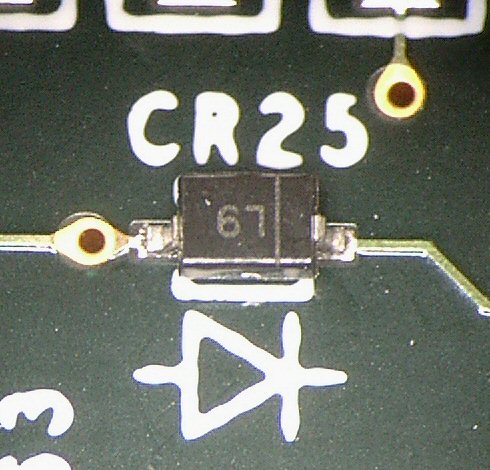
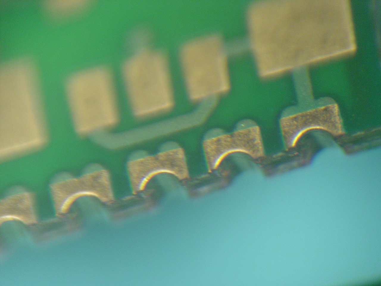
Q: I was reading EDN yesterday, and noticed a picture of a PCB with vias through the pads for 0805 chips. Is this allowed? I guess the solder would fill the via, but who cares, right? What do you suggest?
A: It can be done, but the via must be very small diameter. Otherwise it will tend to 'suck' the solder away from the part and you won’t get a good solder fillet. The pcb manufacturers will offer to fill the vias to prevent ‘thieving’ of the solder for a ‘price’ with conductive epoxy and over plate the top and bottom of the via… This gives you an ‘invisible via’ that takes up no additional real estate on the board, but understand the epoxy material can and will expand at high temperatures and pop the plated tops off the vias, most likely causing a failure. So use this method with caution... More research into via-in-pad technology is called for before going down that road. Notice the lead on the SOT-23 where a via is in the center of the pad...
Do not confuse this with laser vias in pads. They are much more reliable than a plated through hole via in a pad that travels all the way through the board. A laser via usually only goes through one layer of the board to the layer just beneath it. It will not take away solder from the connection.
There is some reading material on-line regarding that type of via. . http://www.laservia.com/library.html
Understand that with each higher level of complexity, you jump a corresponding level in cost. You should consult with the manufacturer before embarking on this sort of design strategy. But it's nice to know it CAN be done, when that is just the solution you need to get your product to market.
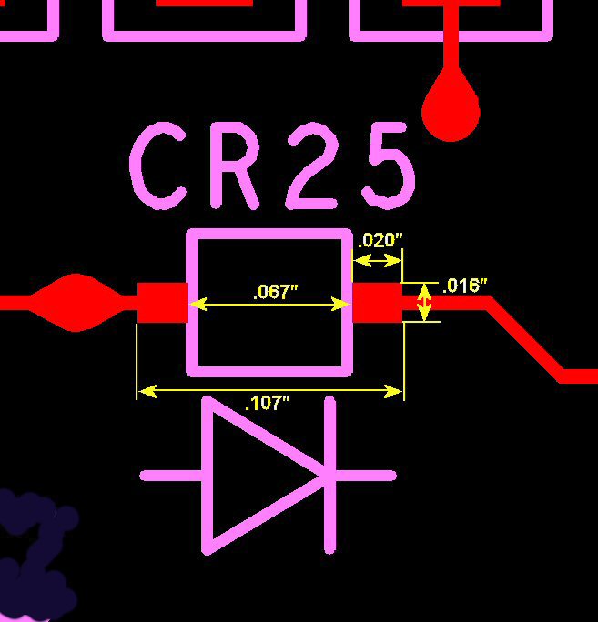
Q: Out of curiosity, is there a recommended clearance between two through-hole solder pads, assuming it is too small to run a trace through.
A: There are no recommended clearances between pads except those driven by design with maybe the sole exception being annular ring requirements for through-hole pads. Even in that instance you are limited only by tolerances.
For example:
There are probably other issues, but I can't think of any at the moment... But, as far as I know, there are no specific rules that say " a through-hole pad must be X amount of distance from any other through-hole pad"... Just make sure the other issues are taken into consideration when spacing them. It is customary, to use a grid to make holes on some finite spacing if you can. But it's not 'required'.
Just use good design practice and your designs should be fine.
Q: Where would I find info on trace spacing based on voltage levels? How far should components be spaced for 1000V vs 4000V that type of thing?
A: Get a copy of IPC-2221 and IPC-2222. Its a good investment in your career. The old "0.0002 in./volt" (0.00508 mm/volt) reference in there originally came from MIL-I-46058. It refers to this being the standard spacing for voltages over 500V between conductors, DC or AC Peak Volts from sea level to 10,000 ft. for an "uncoated board"... Per IPC-ML-910A... and for "coated and internal layers" on a board, according to MIL-STD-275D & IPC-ML-910A it was .00012 in./volt (0.003048 mm/volt). Above 10,000 ft. it says .0010 in./volt (0.0254 mm/volt)
Now I just went to my copy of the IPC 2221 specs, table 6-1 on page 39, and it says basically the same thing... but only in metric, they leave out the inches... (Thanks goes to San Diego Designer Tom Hausherr, CID+, the 'Metric System' promoter for encouraging the IPC to change from inches... The rest of the civilized world uses metric.). I believe IPC has gone all metric so unless you are good at translating... the calculator sounds like a good idea. I have this little windows utility called 'convert.exe' that translates between inches and millimeters for me... I still get it wrong from time to time on my pocket calculator... (I hate when that happens...) I learned in inches and the change over will probably affect me for life... <twitch, twitch> :)
So, for your 1000 Volts AC/DC at sea level to 10,000 ft ASL (3048 m) conductor to conductor spacing on your board should be:
Std 500v spacing 0.1 in.(2.54mm) plus the remainder(1000v-500v)= 500v 500V x .0002 in/volt or .1 inches (2.54mm) add that to the original .1 in. and you get 0.2 inches or (5.08mm)
B1 - Internal Conductors B2 - External Conductors, uncoated, Sea level to 3050m ( 10K ft.) B3 - External Conductors, uncoated, over 3050m ( 10K Ft.) B4 - External Conductors, coated with permanent polymer coating
Note: The IPC-2221 6.3 paragraph refers to insulation between conductors over the board surface and through the dielectric. I would guess this simplifies the spec writing... The dielectric actually has a 750V per mil insulation resistance perpendicular to the layers according to Mil-P-13949/4C for FR4 glass epoxy laminated materials. So 1.3 mils of material perpendicular to the layers would net you 1KV insulation resistance. top to bottom or internal layer to layer. Always give yourself some margin... The back side of the copper foil is rough and can be 'spiked' on the laminated side for adhesion... those spikes and cause the spacing to be less than the minimum target spacing you require when laminated. Also there can be bubbles or voids in the materials that could occur right between your two high voltage conductors... Unless you are trying to mimic a capacitance plane pair, there is little or no reason to have the high voltage lines that close. You don't want a short to occur internally in the board. Give yourself a buffer of at least a couple of layers of prepreg on internal layers.
The chart for 500v for the .00012 per volt section indicates the 500V spacing is .030. Now if you divide .030 by 500v you get .00006 per volt.
So I would say that the .00012 number is not the linear multiplier used to get to the 500V spacing.
They did intend though that you figure out the difference between the 500v and the voltage you are targeting above 500v and add .00012 per volt above 500v to the 500v spacing which is .030.
So for internal or polymer coated traces, at 1000 volts you would need to add .06 to the .03 to get .09 spacing... that's between conductors on the same layer.
For external uncoated traces below 10k ft ASL the spacing is .1 at 500v plus 500v times .0002 which is .1 so you would be at .200 mils for 1Kv.
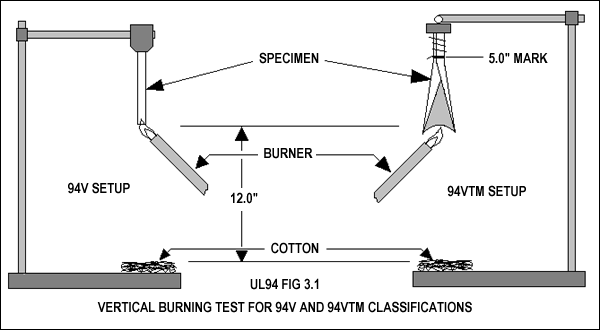
Q: What does it mean when they say that the PCB material must meet UL94 V-0 or better?
A: This is taken from the Boedeker plastics website, see below...
This test uses a ½" x 5" specimen which is held at one end in the vertical position (see Fig. 3.1). A burner flame is applied to the free end of the specimen for two 10 second intervals separated by the time it takes for flaming combustion to cease after the first application. Two sets of 5 specimens are tested. The following are recorded for each specimen:
Table 1. Material Classification
|
|||||||||||||||||||||||||||||||||||||||||||||||||||||||||||||||||||||||||||||||||||||||||||||||||||||
|
|
|
Copyright © 2004 PCB Wizards.COM |
|
|||||||||||||||||||||||||||||||||||||||||||||||||||||||||||||||||||||||||||||||||||||||||||||||||||
| |
||||||||||||||||||||||||||||||||||||||||||||||||||||||||||||||||||||||||||||||||||||||||||||||||||||||