Common design 'mistakes' and recommended solutions
CASE 1) 'A Walk in the
park..... '

Classic mistake, Joe Cool, a Printed Circuit Designer, is greeted in the morning by Johnny Engineer, a cocky graduate of Cal Poly and a gung ho employee of Electronic Widgets incorporated, a prime contractor to the US Navy.
Joe is looking at the schematic and BOM (the Bill of materials) that John put together and sees he has a simple design that should take him about 30 hours to complete. Johnny Engineer bids him 'have a great day' and leaves.... without reviewing the environmental specs.
John didn't think to mention that the board must survive on a JET FIGHTER aircraft and that Joe Designer must layout this board to meet 150 G's of vibration and temperature extremes of -20C to +150C.
Joe Cool Designer goes along his merry way designing the board to the least costly method and chooses material that can only survive to 100 deg C and spaces out the mounting holes at 8 inches apart because he feels there is little reason to use a lot of mounting hardware and they can save money on this design... He then turns in the design on time and under budget, they go for prototype boards. In a week the assemblers are putting it together. Johnny Engineer tests the circuit electrically and it works... Success!
Let's put it in the aircraft and see how it does...

Of course it works just fine after the first test, a quick run down the runway and a return flight and all systems are go... no apparent problems. However they have not done any extensive environmental testing on the boards... but they feel very optimistic and go ahead with the production.
6 months later after the company has built 4,000 boards and shipped them to the Air force, and they promptly install them in the active aircraft for deployment....

Goose and Maverick are over the
Indian ocean at 10,000 feet, the outside temperature
is at 40 deg C ( 104 deg F) which translates to 110 deg C
inside the aircraft body where the
board is in a closed box with no
ventilation and cooling, which starts
to swell the resin/glass board into a
much thicker assembly as it passes
through it's Glass transition phase
after exceeding it's rated temperature.... the weapons system shows a bogie at angels 4 at their six and 'Mav' pulls a high
7g maneuver to put their missiles on target,
and stressing the pc board with 106g's of
vibration.... (well within the target
envelope for this design as
contracted...), and your PCB fails due to a structural crack in the board that severs a
critical signal line at the via hole near U13 that would normally engage the tracking system sensors... but now they fail to operate at the worst possible moment ...
Their 'Goose is cooked'.... your
board failed, and it was completely avoidable.
IF the designer had known in advance
about the environment in which his circuit was to be operated he could have
chosen higher temp board materials and designed the board to survive that environment. Closer mounting holes and many more of them
to make the board more rigid would have cost a little more but the board would have been able to withstand the
intense vibration much better and would not have flexed to the point of failure...


Even normal shipping vibration at a resonance can accelerate components on the surface of the board to over 100g's or 100 times the force of gravity. An aircraft like an F14
or an automobile, or military vehicle can see very high vibration and
extremes in temperature and that can
translate into a very severe
environment for a board to operate in.
Make sure the mechanical engineer has looked at the environmental requirements and defined the board mounting such that no mounting points are farther apart than 4 inches apart in any direction. If you need a board stiffener or some form of vibration restraint or dampener to keep the G forces down on your board, talk about it with the other engineers on your project and make sure that provisions have been made so you do not have a costly redesign or problem later.
Get a copy of IPC-2222 and go over the
materials available for dealing with
higher temperature environments. Ask for the environmental specs before beginning a
design... it could save a life.
Never begin a design without knowing what sort of environment you board must survive and operate within.
According to
Dave S. Steinberg, Steinberg &
Associates, Westlake Village, CA
91361, "The U.S. Air Force
estimates that vibration and shock
cause 20 percent of the mechanical
failures in airborne electronics.
Proper design procedures for ensuring
equipment survival in a shock and
vibration environment are therefore
essential.
Interestingly, the
remaining 80 percent of mechanical
failures relate to thermal stresses
induced by high thermal gradients, high
thermal coefficients of expansion and a
high modulus of elasticity. In both
cases, failures occur primarily from
broken component lead wires, cracked
solder joints, cracking of the component
body, plated hole cracking, broken
circuit traces, board delamination and
electrical shorting."
Know the condition that the board must endure, like the ambient temperature, ventilation, shock, vibration, humidity, thermal limits of the components, susceptibility to molds and fungus, thermal shock or rapid temperature changes, glass transition temperature of the laminate, electrical noise, or susceptibility to RFI (radio frequency interference) such as ECM (Electronic counter measures) or
high power transmitters Jamming and RADAR, High Voltage or High Current requirements, etc. the list can be very long...
(By the way...if you didn't guess, the
scene you just witnessed was entirely
possible, but was completely
fictitious... this was all a
fabrication of my wild imagination...
but it could happen to anyone that
fails to do their homework... Don't
get caught unprepared...)


CASE 2) How much is "That
much?"
Joe Cool, our favorite designer, is working on a board and has a new component to layout. He needs to design a footprint for this component, a quad flat pack chip made by XILINX. Joe gets a copy of the datasheet for the component from the electrical engineer and reviews it for any recommended footprint data... he finds none. So he starts to create a foot print from the mechanical data in the spec.
First he looks for the PITCH or 'lead to lead spacing' of the leads on the component. Then the distance from row to row in both directions and finally the component body size, so he can make a silk screen pattern to show the component orientation for assembly. Joe makes all the pads for the leads as close to the actual size of the 'foot'' of the lead as he can, wanting to make as much routing space as possible available for later routing of the board...
All the dimensions are nominal, exactly as the dimensions are shown on the data sheet. Joe routes his board by first fanning out his power connections and then running the router on the remaining traces to get 99% complete routing. He only has to route a single line by hand... terrific!
He runs the Gerber files and ships the files to his favorite board vendor to make the boards...
A week later the assembly guys are placing his board, and lo and behold.... the new IC chip does not fit!
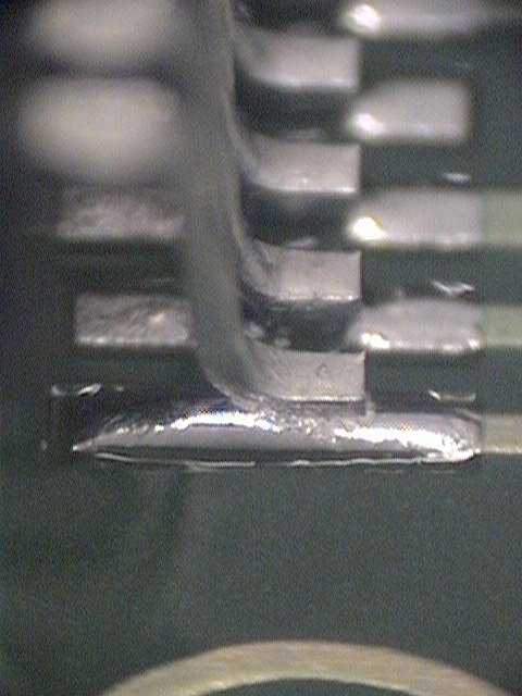
What did Joe Cool forget?
All physical objects are not 'perfect'. Things are constantly changing size and shape all the time. Mostly due to
humidity and temperature... As things get hotter, they expand,
when they get colder they shrink or contract. Some materials have wide variations in size due to temperatures,
in other materials the changes are so
small or minute that it is hard to measure a difference.
When products like IC's are manufactured, they are affected by the inaccuracies in the equipment that form the leads and the molds that make the ceramics or plastic bodies of the parts... All data sheets should contain the
LMC least material condition and the
MMC maximum material
condition
of any physical part of the IC. Some times these are expressed in min/max values, other times they are in +/- tolerances. Be aware that you must account for these variations when designing a part footprint.
You can read more about Geometric
Tolerances in the IPC specification
IPC-2615 Printed Board Dimensions and
Tolerances.
Always remember to allow for the maximum size the part can be and the minimum size the part can be, allow for the tolerances of the machine that places the part on the board, allow for the over etch or under etch of the conductor pads and traces, and the positional tolerance of the multilayer etch patterns for one layer to another... These tolerances will make the footprint size grow to accommodate these component variations and drive the geometries you must use to make a repeatable,
producible product.
Also, don't fall into the trap of 'round off' values in CAD systems. Some older CAD products only had resolutions of 1 mil... so doing a footprint with a finer resolution was a
'round off' challenge. If you assumed that the distance was the same between each component lead and it was off by .0005 inches , after placing the 25th lead you would be off by 12.5 mils!
Accumulated Tolerance buildup.... will mess up your design every time unless you account for it... Build your footprints at 1:1 scale and always allow for
the tolerances.
TBD...