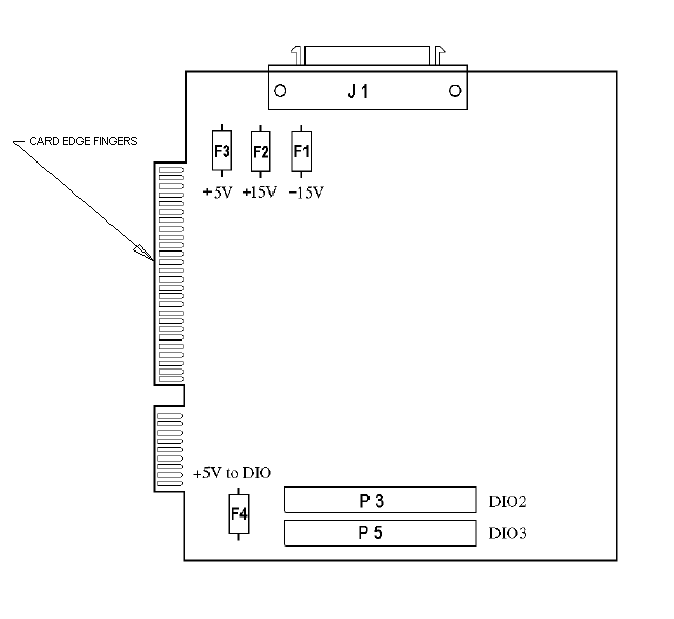
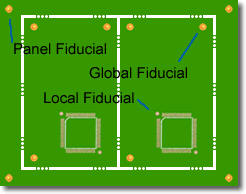
Global Fiducials:
Fiducial marks used to locate the
position of all features on an
individual printed circuit board.
When multiple boards are processed
as a panel, the global fiducials
may also be referred to as panel
fiducials if used to locate the
circuits from the panel datum.
Local Fiducials:
A fiducial mark (or marks) used to
locate the position of an
individual land pattern or
component that may require more
precise location, such as a .020”
pitch QFP.
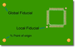
Image Fiducials:
Global fiducial marks on a multiple
printed circuit board fabrication
panel that are located within the
perimeter of an end-product printed
circuit board.
Panel Fiducials:
Global fiducial marks on a multiple
printed circuit board fabrication
panel that are located outside the
perimeters of the end-product
printed circuit boards.
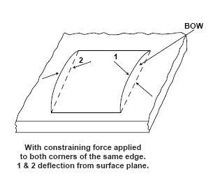
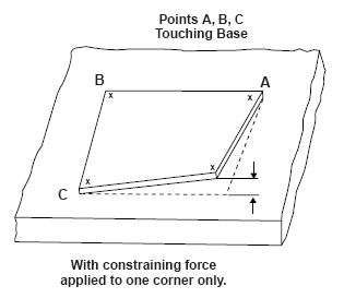
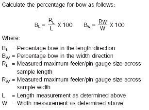
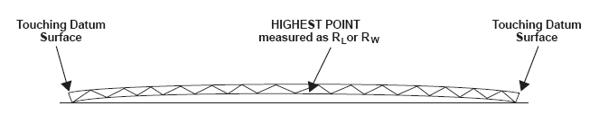
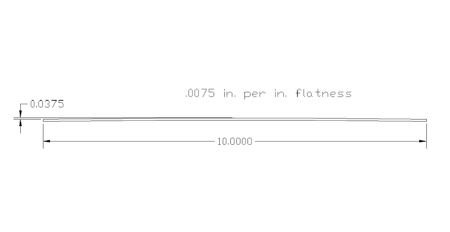
Flatness:
Board flatness is described in
terms of a deviation from a
theoretical perfectly flatness in
inches square... with the effective
deviation from that datum being
.0075 in per in for surface mount
technology boards. (Through hole
technology allows .0150 in. per in.
deviation). What that means is that
any given square inch of board
surface will not exceed a
difference of .0075 inches in it's
flatness with respect to any
adjacent square inch of board
surface around it. An example of
this would be like the figure shown
below, where we have a board that
is 10 inches wide and is
illustrated in a typical arc at the
extreme bow or warp that still
would pass under the .0075 in. per
in. rule. The total deviation for
the board at it's center is only
.0375 inches from edge to center
assuming the maximum allowable
deviation inch per inch across it's
surface from end to end.
For the specification regarding
testing for surface flatness see
IPC-TM-650 Method
2.4.22.
http://www.ipc.org/4.0_Knowledge/4.1_Standards/test/2.4.22c.pdf