Thermal Relief Pad
- AKA Thermal Ties, Wagon
Wheels, Thermal Webs
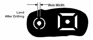
Thermal
connections to a plane are described in
MIL-STD-275E paragraph 5.2.5 Thermal
Relief in Conductor Planes
and referenced in Figure 14 'Ground
Plane Lands' in the Appendix. IPC
has since replaced MIL-STD-275 with
IPC-2221 and IPC-2222. There in section
9.1.3 of IPC-2221 you find the same
information as was published in
MIL-STD-275 with a reference to IPC-2222
the 'Sectional standard' for 'more
detailed information'...
Regarding the
IPC-2222 9.1.2 Thermal Relief in
Conductor Planes you will find
the relationship between the hole size,
land and web area is has a very specific
relationship which they choose to term as
'critical'.
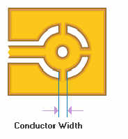
Typically, to calculate
the width of the thermal tie connections
you need to divide the minimum land area
diameter by 60% and then divide that
number by the number of spokes desired to
obtain the width of each thermal
connection trace.
Example:
LAND SIZE CALCULATION
Maximum hole size = 1.0 [0.040]
Annular ring = 2 x 0.13
[0.005] = 0.26 [0.010]
Fabrication allowance = 0.25 [0.010]
Minimum land size = 1.0 [0.040] +
0.26 [0.010] + 0.25 [0.010] = 1.51
[0.060]dia.
THERMAL RELIEF CALCULATION
Total thermal width = 60% of land size
= 0.6 x 1.51
[0.060]
= 0.91 [0.036
ORIGINAL WEB SIZE CALCULATION
2-web width = one-half of total thermal
width
= 0.5 x 0.91 [0.036]
= 0.45 [0.018]
3-web width = one-third of total thermal
width
= 0.33 x 0.91 [0.036]
= 0.30 [0.012]
4-web width = one-fourth total thermal
width
= 0.25 x 0.91 [0.036]
= 0.23 [0.009]
The total
cumulative copper in the spokes for all
layers in any plated thru hole must not
exceed 160 mils or 4.0mm for 1 oz.
copper... 80 mils or 2.0mm for 2oz
copper.
Also you
need to make sure that you do not
restrict the current carrying capacity of
the plated thru hole structure by
removing too much copper.
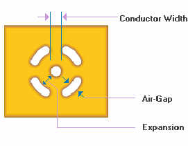
If the land size used in the design is
greater than the minimum value calculated
above, then the percentage difference
between the land diameters must be
subtracted from the total web width
calculation. This balances the
thermal distribution in the pad
compensating for the greater copper
volume in a larger than minimum pad.
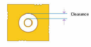
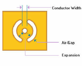
The next consideration is the clearance
area between the land and the copper
plane. Section 9.1.3
Clearance Areas in Planes, points
to an illustration that clearly states
that the clearance area should not be
less than 10 mils or 0.25mm and/or not
less than the electrical spacing
requirement based upon the voltage being
applied to the conductors.


